
For training, please contact the Tool Manager(s).
Training takes 1 hour and is hands on. Bring your substrate.
- All material must be approved by tool manager.
- No halogenated polymers like polyvinyl chlorides (PVC, PVDC) or fluropolymers (teflon)
- No polypropylenes
- No foils
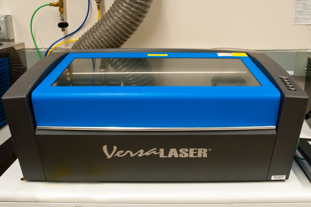
The Universal Laser Systems VersaLaser VLS3.50 is a CO2 laser that emits in the infrared spectrum to cut or etch patterns by vaporizing the substrate. The tool is equipped with optics that focus to spot sizes of 25.4 or 127 microns. The tool accommodates substrates up to 24 x 16 inches and several inches thick.
The laser is controlled by CorelDRAW or AutoCAD plotting software. Designs are translated into varying depths, widths, and edge qualities. Cuts with microscale widths as small as 35-120 microns (depending on the substrate)can be achieved.
Substrates that can be CUT through include: heat-resistant glass (borofloat & fused silica are best), some plastics/polymers, mylar, nylon, papers, some rubber, PDMS (silicone).
Sapphire substrates can be cut with care.
These materials as well as many metals can be ENGRAVED. Silicon nitride can be etched, somewhat.
Unfortunately, silicon wafers and metals such as gold, aluminum and brass are impervious.
Users have reported success with the following:
- through holes & channels in glass & quartz wafers for anodic bonding or other uses
- microtoroid fabrication in thin layers of silicon oxide
- micromachining plexiglass & PMMA for molds or parts
- rapid prototyping of polyimide or kapton tape devices
- precision-cut rubilith masks
- cutting gaskets & seals in rubber or double-sided tapes
- direct cutting or etching of PDMS
- marking metals & silicon wafers with metal marking compounds
- creating simple paper-based microfluidic devices & stencils
- microfluidic channels in polymers (Zeonor, PMMA, PDMS, acrylic)
- Shadow masks and rubilith masks
- microfluidics
- Plexiglass containers
- Ports
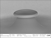
An optical resonator made from a silica microtoroid with extremely smooth side walls that enable very narrow optical resonances. The microtoroid was fabricated by defining a 100 micron-dia. silica disk on the top of a silicon wafer, undercutting the rim with a xenon difluoride isotropic etch, and partially melting the overhanging rim with the Versalaser. The infrared light was absorbed by the silica, but passed through the silicon, melting the edges without affecting the underlying substrate. (Fabricated by David Hutchison, Applied Physics, PhD candidate, 2011).
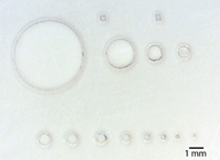
Array of through holes (100-5000 microns dia.) in a 500 micron-thick fused silica wafer. Holes were cut with minimal damage to the edges by repeated, low-intensity passes of the laser. Typical settings allow a 1000 micron-dia. hole to be cut in under 20 seconds. Subsequent CMP processing can prepare the cut wafer for anodic bonding.