Training for the furnace area covers the pre-furnace MOS clean, atmospheric and LPCVD processes. It is scheduled on a need basis, please email the tool manager for training requests. Include MOS area training in the subject header. You will be notified when the next scheduled training will be by email.

Description

Furnaces for growing silicon oxide and depositing polysilicon, silicon nitride, and silicon oxide as well as processes for cleaning the wafers before deposition.

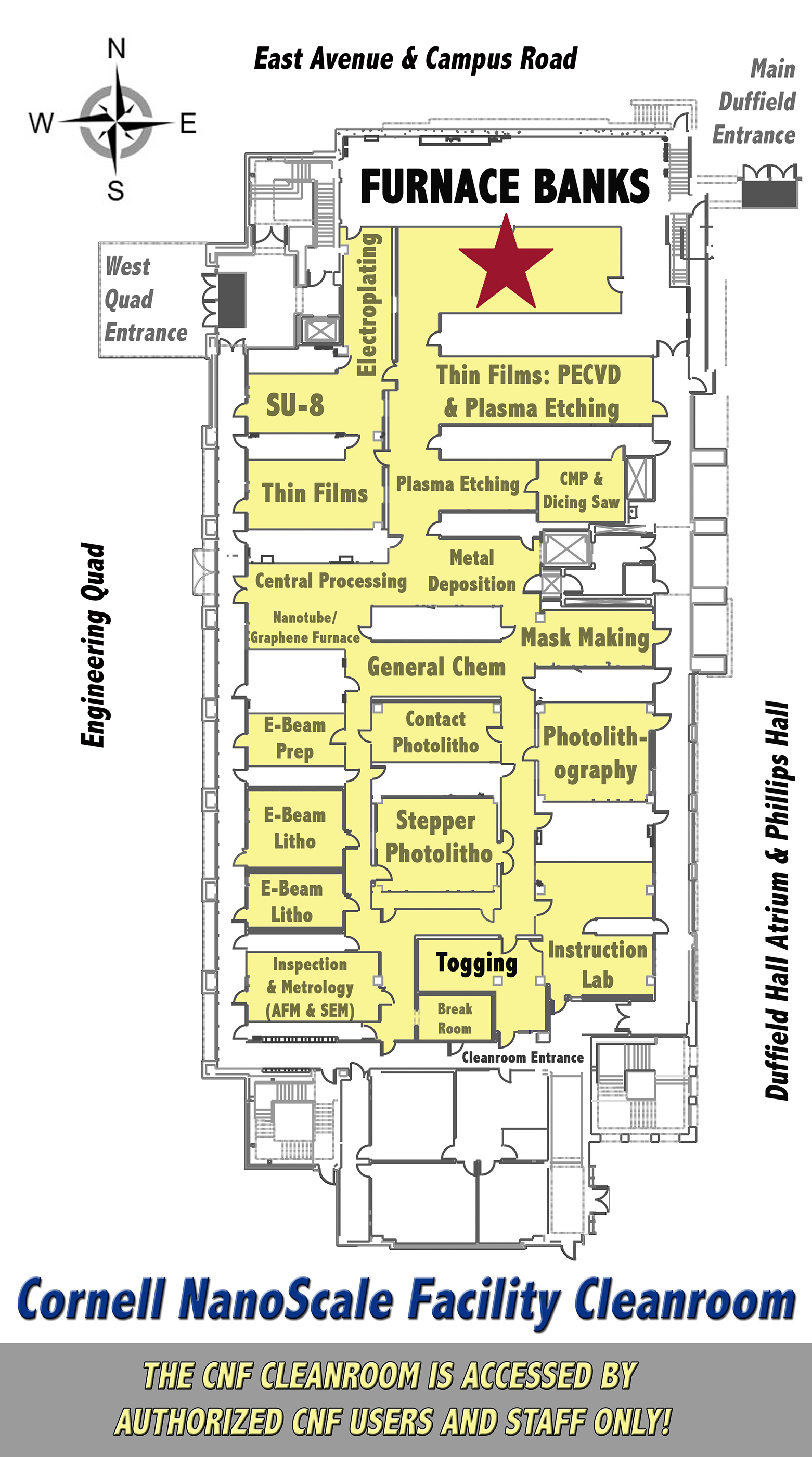
A1 - General Material Anneal 1

The Anneal 1 Furnace is an atmospheric furnace with a 42” flat zone capable of processing up to 6” diameter wafers. The furnace tube is equipped with N2 and Ar gases for inert ambient processing,  O2 for dry oxidation, and pyrogenic steam for Wet Oxidation processes.  Most sample materials are accommodated.

A2 - POCL3 Doping

The POCL3 Furnace is an atmospheric furnace with a 42” flat zone capable of processing up to 6” diameter wafers. The furnace tube is equipped with an POCL3 liquid bubbler, O2 for doping processes, dry oxidation and O2/inert mixtures, as well as an N2 anneal ambient.

A4 - LPCVD Silicon Carbide

The 

The LPCVD Siliocn Carbide Furnace is an atmospheric furnace with a 42” flat zone capable of processing up to 6” diameter wafers. Process gases available are Dichlorosilane, acetylene, Hydrogen and Ammonia.  Undoped poly-crystaline silicon carbide and nitrogen doped silicon carbide can be deposited.

B2 - Wet/Dry Oxide

The Thermal Oxidation Furnace is an atmospheric furnace with a 40” flat zone capable of processing up to 6” diameter wafers. The furnace tube is equipped with an external torch for pyrogenic wet oxidation, high and low O2 flow controllers for dry oxidation and O2/inert mixtures, as well as N2 and Ar anneal ambient. Samples are restricted to silicon based materials only.

B3 - LPCVD LTO

The LPCVD Low Temperature Oxide furnace is a low pressure CVD furnace with a 40” flat zone capable of processing up to 6” diameter wafers. Process gases used are SiH4 and O2. Samples are restricted to silicon based materials only.

B4 - LPCVD Silicon Nitride

The LPCVD Silicon Nitride furnace is a low pressure CVD furnace with a 40” flat zone capable of processing up to 6” diameter wafers. Process gases used are SiH2Cl2, NH3, and N2O. CVD silicon nitride films with controlled stress and high temperature oxide (HTO) can be deposited. Samples are restricted to silicon based materials only.

C1- MOS Metal Anneal 3

The Anneal 3 Furnace is an atmospheric furnace with a 40” flat zone capable of processing up to 6” diameter wafers. The furnace tube is equipped with N2 and Ar gas for inert ambient processing, H2 for forming gas mixtures, and O2 for dry oxidation with or without HCL. Samples are restricted to silicon based materials and a limited set of approved metal films.

C2 - MOS Metal Anneal 4

The Anneal 4 Furnace is an atmospheric furnace with a 40” flat zone capable of processing up to 6” diameter wafers. The furnace tube is equipped with N2 and Ar gas for inert ambient processing, H2 for forming gas mixtures, and O2 for dry oxidation with or without HCL. Samples are restricted to silicon based materials and a limited set of approved metal films.

C4 - N+/P+ Polysilicon

The LPCVD Polysilicon Furnace is a low pressure CVD furnace with a 40” flat zone capable of processing up to 6” diameter wafers. Process gases available are SiH4, N2/PH3 and N2/B2H6 mixes for insitu doping, HCL for cleaning. Samples are restricted to silicon based materials only.

D3 - CMOS N+ Polysilicon

The CMOS N+ LPCVD Polysilicon Furnace is a low pressure CVD furnace with a 40” flat zone capable of processing up to 6” diameter wafers. Process gases available are SiH4, He/PH3 mix for in-situ doping, and HCL for cleaning. Samples are restricted to silicon based materials only and CMOS restricted tools and films.

E4 - LPCVD CMOS Nitride

The LPCVD CMOS Silicon Nitride furnace is a low pressure CVD furnace with a 40” flat zone capable of processing up to 6” diameter wafers. Process gases used are SiH2Cl2, NH3, and N2O. CVD silicon nitride films with controlled stress and high temperature oxide (HTO) can be deposited. Samples are restricted to silicon based materials only and CMOS specific tool and film limitations.