
Currently, this fully automated tool does not allow hands-on users. Interested users can contact the manager of the High Frequency Test Lab to arrange for normal configuration/custom setup and sample loading/unloading. Through a personal computer, users can then remotely control the measurements. For automated stepping across hundreds or thousands of devices on a wafer, users need to purchase their own probes, because the probes can quickly wear out. For testing just a few devices with probe pads of 50-um pitches, HFTL's existing 220-GHz probes can be used. Probes at lower frequencies and different pitches are also available, but require custom setup.
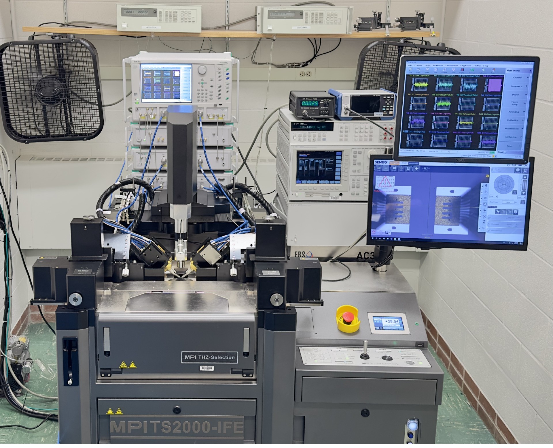
The tool is based on an MPI TS2000-IFE 200-mm automated probe station with micron precision. In the standard configuration, the tool includes two RF probes of GSG, GSSG or GSGSG types, a microscope, a digital camera, and a thermal chuck with temperature control between -60°C and +200 °C. Other DC and RF probes may be added. The probes, the microscope, and the chuck are all automatically controlled in x, y, and z directions with optical feedback. The RF signal is provided by an Anritsu 4-Port ME7838G vector network analyzer capable of a single sweep from 70 kHz to Fig. 2. HFTL Terahertz small-signal 220 GHz. Up to 12 DC bias can be supplied by an Agilent 4156C probe station precision semiconductor parameter analyzer capable of +/-200 V, 0.5 A, and 100 V/us pulses, and two Agilent 6629A system DC power supplies capable of +50 V and 2 A. The tool is fully automated as controlled by MPI Sentio, MPI QAlibria, and Keysight IC-CAP software.
- Anritsu ME7838G Vector Network Analyzers, 70 kHz to 220 GHz, 4-port single sweep
- Singled-ended GSG and differential GSSG and GSGSG measurements
- MPI TS2000-IFE 200-mm automated probe station with micron precision and -60°C to +200 °C temperature control
- Agilent 4156C precision semiconductor parameter analyzer capable of +/-200 V, 0.5 A, and 100 V/us pulses
- Agilent 6629A 50W system DC power supply, +50 V, 2 A
- Pulsed RF transient measurements before, during, and after the pulse
- Large-signal nonlinear measurements such as gain compression, spectrum analysis, harmonic/intermodulation distortion
- VDI frequency extenders can be added to extend the power and frequency range