Zeiss Ultra and Supra SEM Training:
First, complete the SEM video training course RSRCH - CNF - SEM101 in Workday Learning.
Next, let us know you finished the Workday Learning course and request training, by sending an email to the CNF SEM team.
Please do not come to the training unless you have a sample ready to image. You will be required to use the SEM within one week of training or your access may be removed.
- Fully Baked Resist Only!
- Samples should be cleaned and baked before imaging
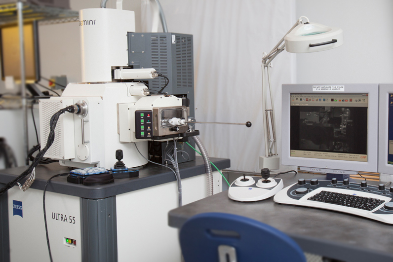
Scanning electron microscopy is critical for the analysis of nanoscale materials and structures. CNF operates two field emission scanning electron microscopes (SEMs): a Zeiss Supra 55 microscope capable of variable pressure (VP) operation and a Zeiss Ultra 55 microscope optimized for high resolution imaging. Like most modern SEMs, both systems are capable of operating at beam energies from 100 V to 30 kV. However, the unique electron optical design employed in the Zeiss systems enables unsurpassed performance at beam energies from 100 V to 8 kV. This is crucial for obtaining high resolution distortion free images of surface.
The Ultra 55 is designed to maximize imaging resolution at low beam energies. It is equipped with a backscatter electron detector engineered to image electrons with energies less than 2 keV. An energy filter incorporated into the detector enables energy selective backscatter (ESB) imaging. This signal can be used to obtain contrast between regions of different composition.
- In Lens Energy Selective Backscatter (ESB) Detector
- Backscatter imaging using 100 eV to 3 keV beam energies
- In situ electrical characterization of samples using the installed Zyvex system