SubTitle
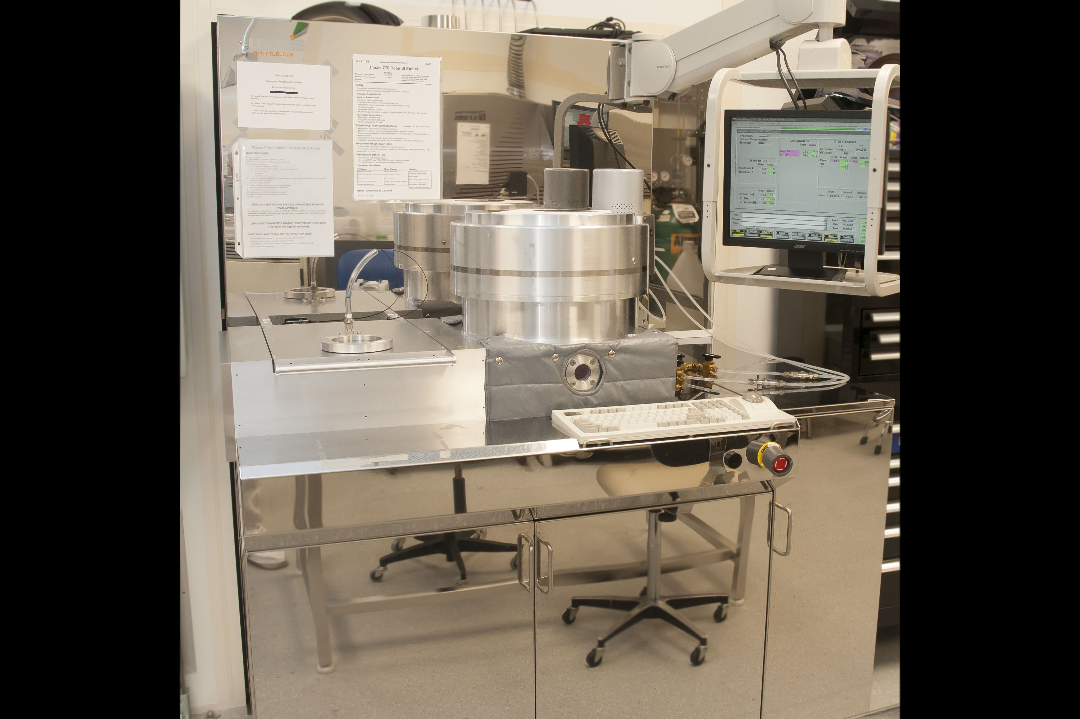
Bosch Etcher for deep silicon etching
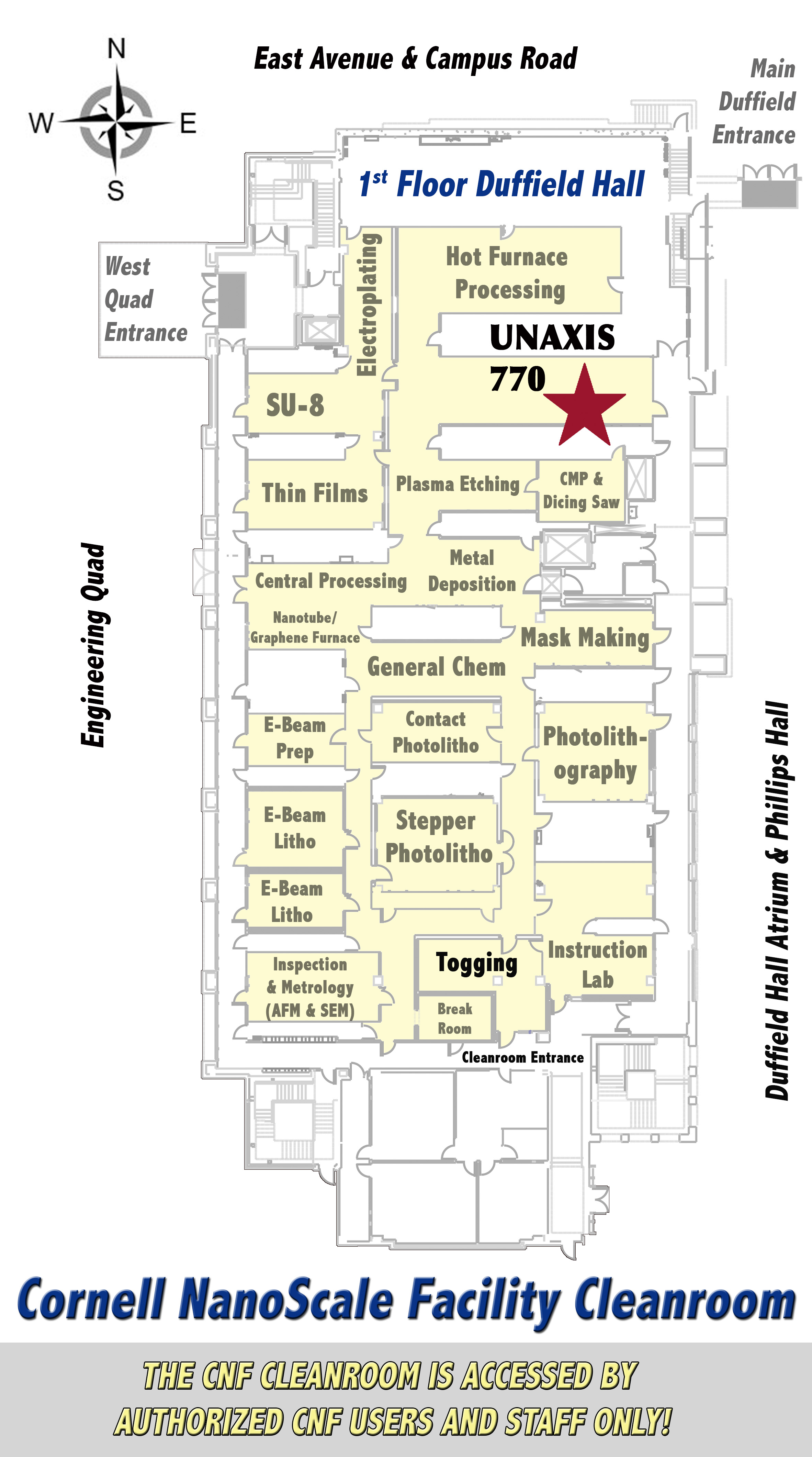
Tool Location
107
Training
For training, please contact the Tool Manager(s).
Compatibility:
Additional Restrictions
- Whole 4 silicon wafers and pieces mounted to sapphire wafer
- Thermal Oxide, Photoresist or Alumina (Al2O3) masks only
- Photoresist masks require edge bead removal (> 5mm around entire edge of wafer)
- No other polymers or adhesives
- No metals exposed to the plasma.
Manager
Backups:
Body
A single chamber (licensed Bosch fluorine process) inductively coupled plasma / reactive ion etcher, the Unaxis SLR 770 etcher is used to etch deep patterns in single crystal silicon substrates. The resulting features are used for MEMS and biological applications. Etch rates of up to 2 microns per minute and aspect ratios of 20:1 can be obtained using photoresist or silicon dioxide as a masking medium. Photonics etch for shallow silicon etching is available as well.
Capabilities
- Load Locked sample introduction
- 4 inch and 6 inch silicon wafer capability. Users wanting to etch 6 inch silicon wafers need to contact the tool manager.
- High selectivity single crystal silicon etch with resist masking
- Through wafer single crystal silicon etch with silicon dioxide masking
Processes Available
Bosch process for deep silicon etching.
Photonics etch (C4F8/SF6) for shallow silicon etching.