
First, complete the SEM video training course RSRCH - CNF - SEM101 in Workday Learning.
Next, let us know you finished the Workday Learning course and request in-person training, by sending an email to the CNF SEM team.
- Fully Baked Resist Only!
- Samples should be cleaned and baked before imaging
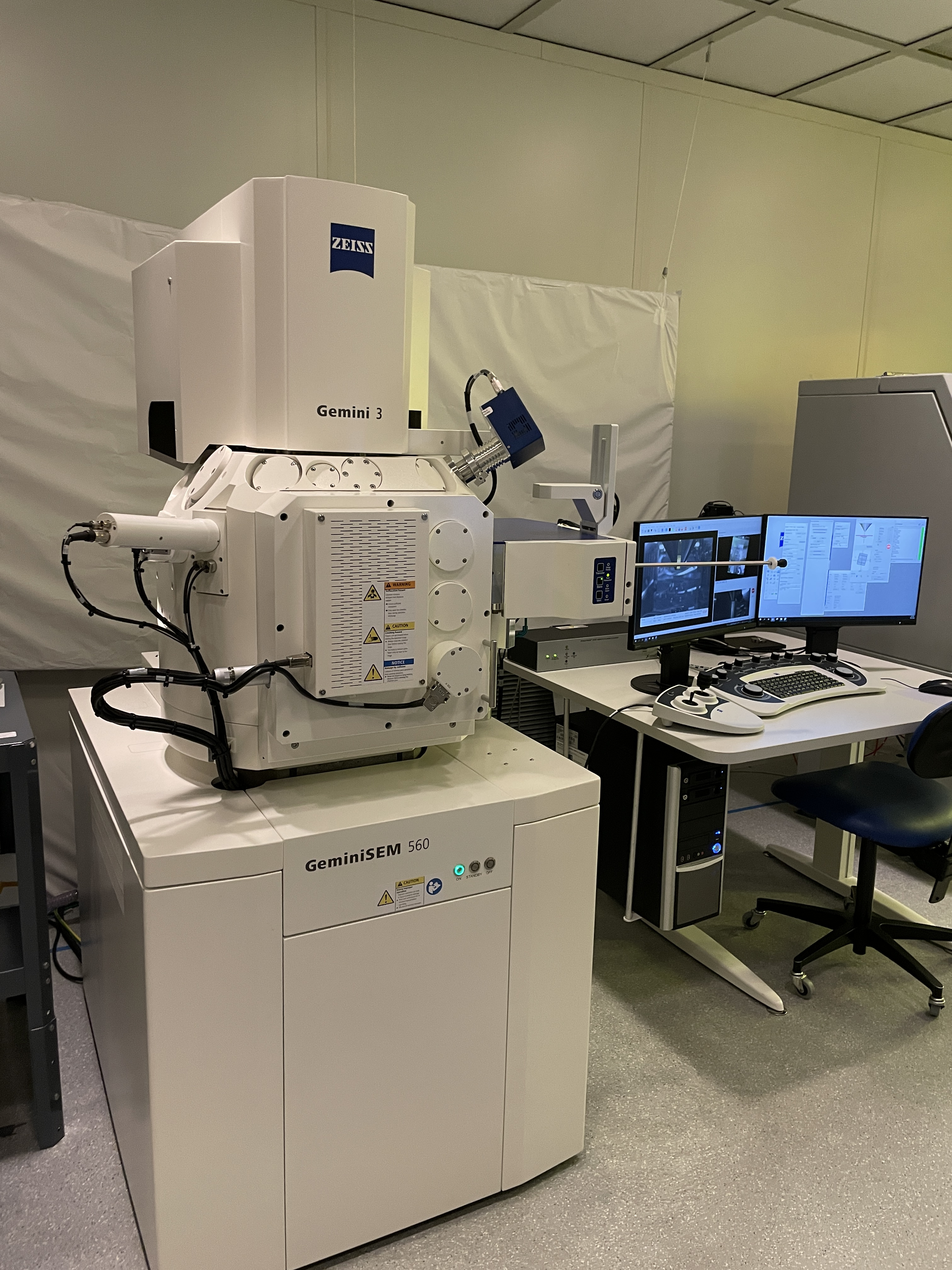
Scanning electron microscopy is critical for the analysis of nanoscale materials and structures. CNF operates three field emission scanning electron microscopes (SEMs). ZEISS Gemini SEM stands for effortless imaging with sub-nanometer resolution. Take sub-nanometer images below 1 kV without an immersion lens. All systems are capable of operating at beam energies from 50 V to 30 kV.
The Gemini SEM accommodates large samples with ease, while its load lock enables efficient transfer of up to 8-inch wafers. A key feature of this instrument is its integrated navigation camera. This capability allows users to efficiently locate regions of interest and perform seamless edge-to-edge examination across full 8-inch wafers.
- 0.8 nm resolution at 1 kV
- 0.5 nm resolution at 15 kV