For training, please sign up in Workday Learning for course:
- RSRCH - CNF - Schott IR Inspector
- Do not use tacky or wet chemistry on substrate while operating the tool.
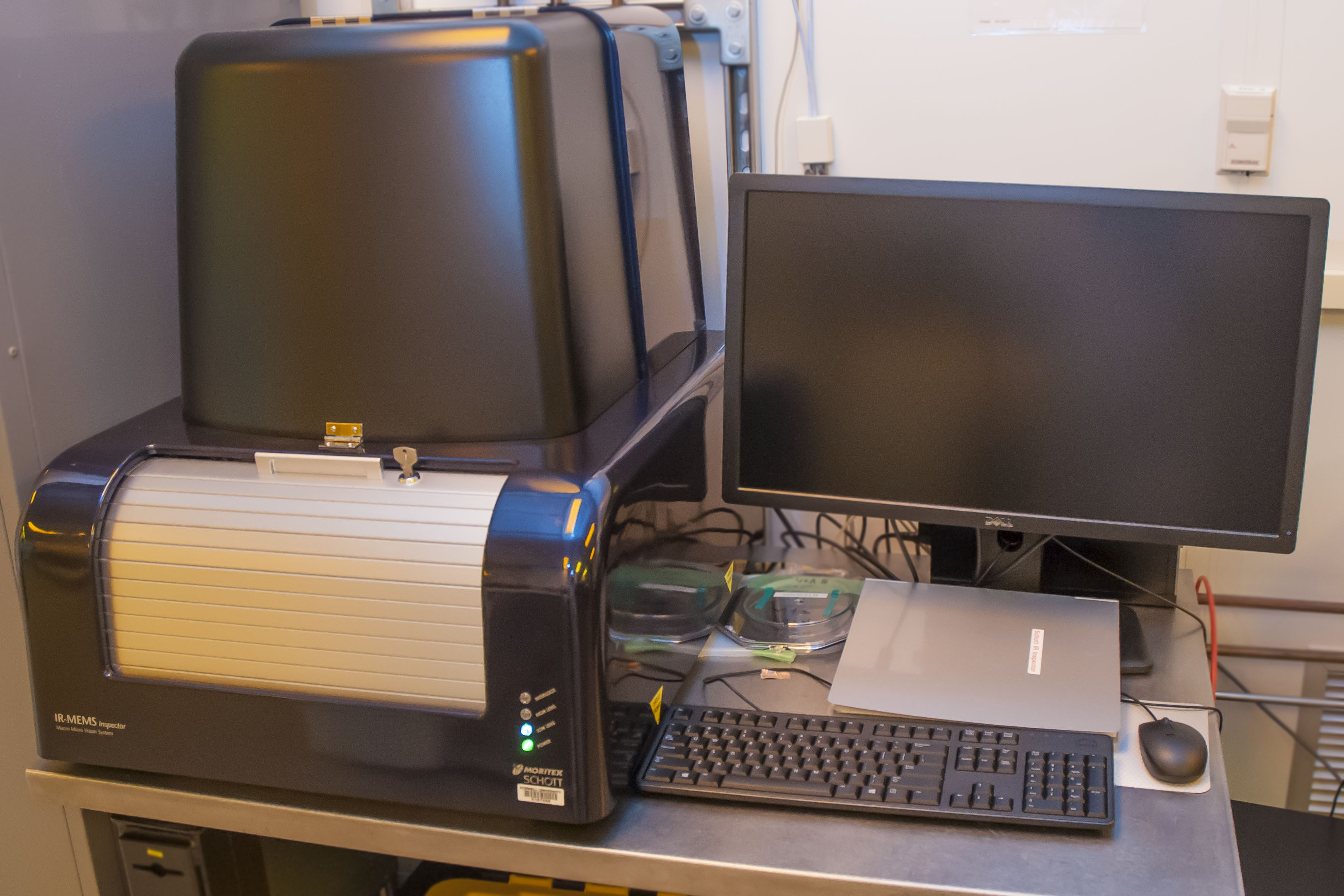
The Schott IR Inspection Tool is a general all purpose semi-automatic inspection tool for front side, buried layers, and backside inspection. The machine can handle substrates size up to 200mm in Diameter.
Buried layers in bonded silicon wafers can be imaged with this tool due to its infrared camera.
Currently a low-mag camera is operational.
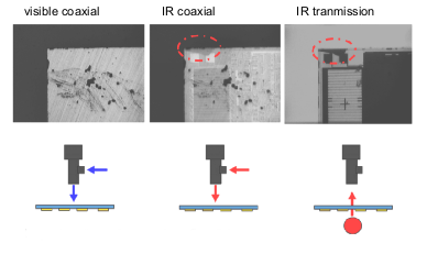
The Schott IR Inspection currently has three illumination modes; near infrared coaxial illumination, near infrared transmission and near infrared oblique illumination. Other illumination sources can be added in the future. These modes give the machine sub-micron resolution for a variety of applications.
The Schott IR Inspection has two main magnification operational modes; low magnification that ranges from .75x to 4.5x and high magnification that ranges from .7x all the way to 40x. The field of view for those modes ranges for low magnification between 7.09 x 8.88mm to 1.18 x 1.48mm and for high magnification from .71 x .89mm to .13 x .17mm.
- Low Magnification Mode using Coaxial Illumination for visible, UV or IR.
- Low Magnification Mode using off axis Dark Field Illumination for visible, UV or IR light.
- Low Magnification Mode using Backside Dark Field for IR.
- Low Magnification Mode using Backside Bright Field for IR.
- High Magnification Mode using Coaxial Illumination for visible, UV or IR light.
- High Magnification Mode using off axis Dark Field Illumination for visible, UV or IR light.
- High Magnification Mode using Backside Dark Field for IR.
- High Magnification Mode using Backside Bright Field for IR.
The Schott IR Inspection can be utilize for void detection and quality of bonds in wafer bonding. In terms of wafer packaging it can be used to inspect interconnects in single layer or in multilevel designs. It also serves as a good way to detect chipping and cracking post-CMP and post-Dicing for top and buried layers. This machine is capable of processing substrates very quickly. Processing time is dominated by image magnification and the size of the substrate. Image stitching and file size are inversely related to those two factors. The Schott IR Inspection ’s broad optical zoom range makes it ideal for layer characterization pre-processing and post-processing. Image storage is available locally on the machine and on the local CNF network.
Silicon is opaque to visible light which has a wavelength range from 400 to about 700nm. Infrared light in the other hand has a longer wavelength of about 1100nm. At this wavelength silicon become transparent. This is due to silicon having a bandgrap of about 1.1 eV. Then bandgap is the energy range in solids where no electron can exist. This is located between the valence band and the conduction band. Schott takes advantage of this phenomenon to image buried layers when Silicon is the predominant layer. The Machine is sensitive to:
Si-Si, Si-Glass, Si-Au, Si-GaGs, Si-GaP, Si-GaAsP, Si-LiNbO3, Si-LiTaO3, Si-Au-PZT, Si-Au-PLZT, Si-polymer-Si.