SubTitle
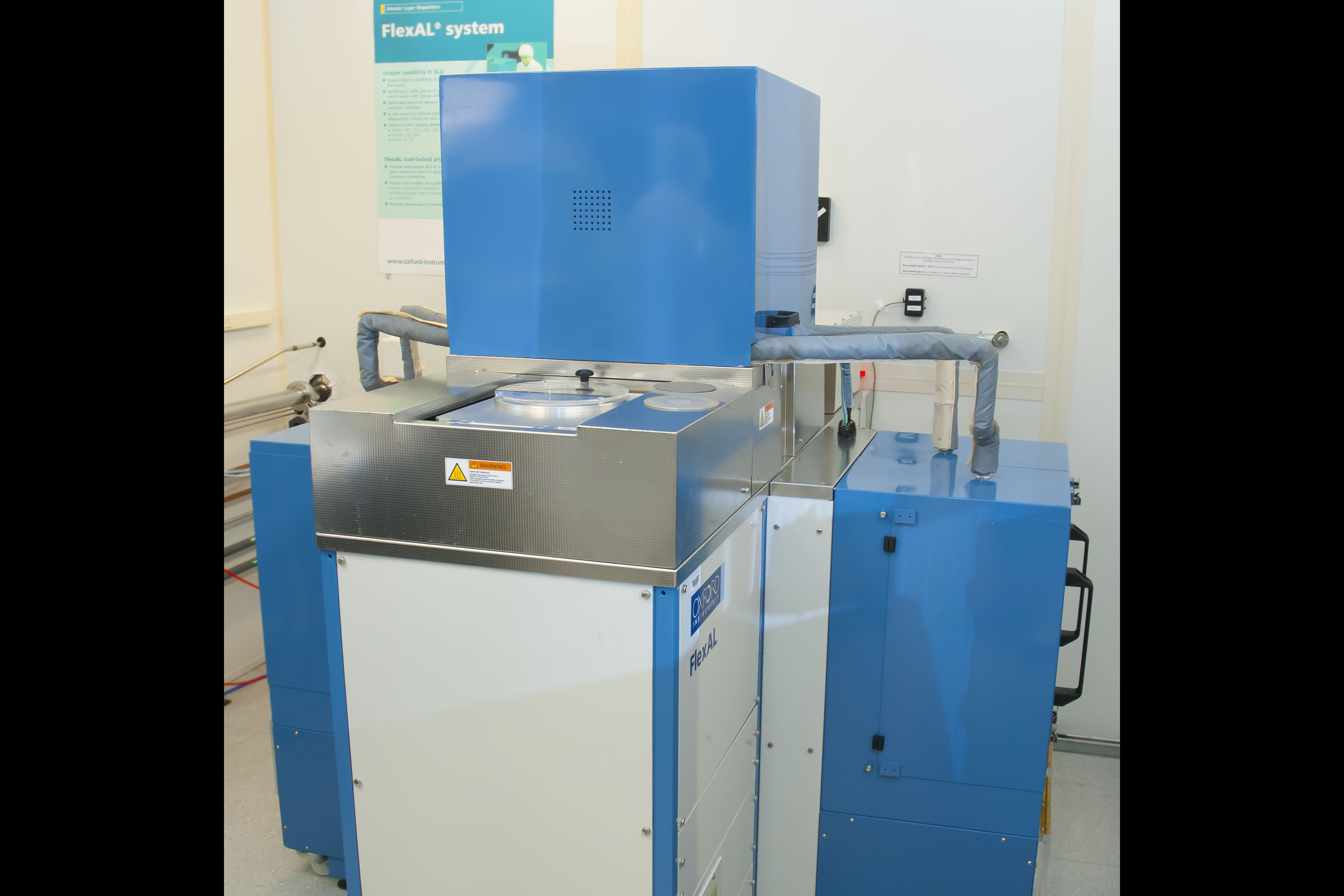
Atomic Layer Deposition
Tool Location
103
Training
For training, please contact the Tool Manager(s).
Compatibility:
Additional Restrictions
- No films thicker than 50nm or 500 loops without permission of the tool managers
- No changing of recipes other than loop count without permission of the tool managers
- Full size 100mm wafers (other wafer sizes up to 200mm can be accommodated with staff assistance).
- Pieces can be processed with the use of the dedicated Aluminum carrier plate.
- Polymers and resist need to be fully cured and only run using 110C processes
Manager
Backups:
Body
Atomic Layer Deposition (ALD) offers the opportunity to create precisely controlled structures for advanced semiconductor and other nanotechnology applications, by creating ultra-thin films on nanometre and sub-nanometre scales. A unique property of ALD is its ability to deposit material conformally into high aspect ratio features. The technology is widely regarded as a key enabler of the next generation of smaller semiconductor devices.
Capabilities
Available thin film materials:
- Al2O3-plasma and thermal
- AlN-plasma
- HfO2-plasma and thermal
- HfN-plasma
- TaN-plasma and thermal
- Ta2O5-plasma and thermal
- SiO2-plasma
- Si3N4-plasma
- HfAlOx-plasma
- HfSiOx-plasma
- HfSiOxNy-plasma
Applications
These highly uniform thin films (<50nm) can be used as high-k dielectrics and metal gates for advanced transistor fabrication, along with applications to MEMS/NEMS and photonics applications.
Resources: