SubTitle
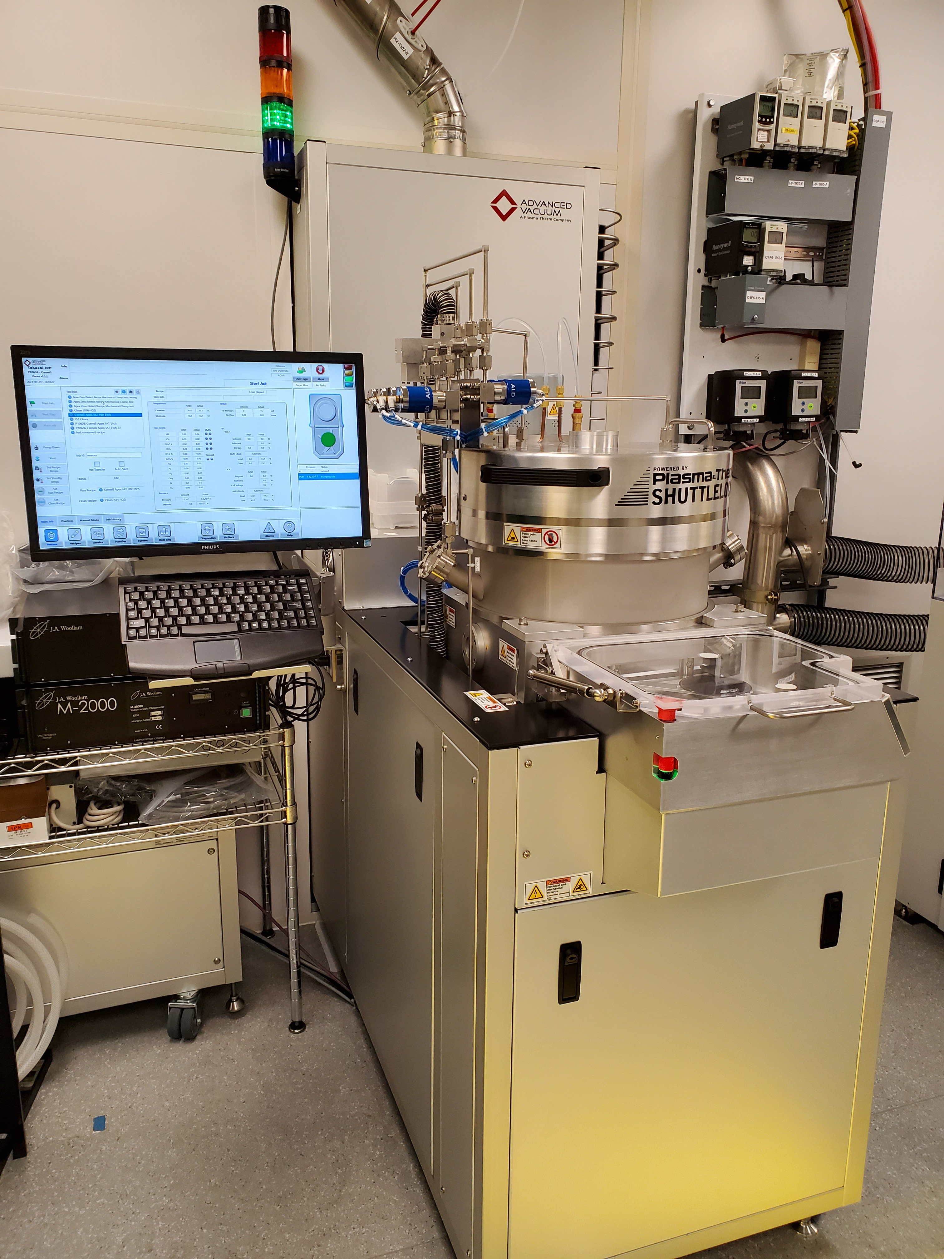
Atomic Layer Etching
Tool Location
110
Training
For training, please contact the Tool Manager(s).
Compatibility:
Additional Restrictions
Select III/V materials allowed- ask staff before proceeding!
Manager
Backups:
Body
Atomic Layer Etching system configured with an ICP and loadlock