
TRAINING
After a user has done the general electron beam lithography training described at https://www.cnfusers.cornell.edu/Electron-Beam%20Lithography , this training covers operation of the JEOL 6300 (JEOL 9500 training is separate from JEOL 6300 training).
Training on the JEOL 6300 takes place in the cleanroom. Please send email to ebeam (at) cnf.cornell.edu to request training.
IF YOUR E BEAM EXPOSURE WILL BE ALIGNED WITH A PATTERN ALREADY ON THE WAFER, PLEASE READ AND FOLLOW THE DIRECTIONS AT https://www.cnfusers.cornell.edu/ebeam_alignment BEFORE DESIGNING ANY DEVICE PATTERNS IN CAD. NOT FOLLOWING THESE DIRECTIONS MAY MAKE ALIGNMENT IMPOSSIBLE.
- Whole silicon wafers only - discuss pieces or other materials with managers.
- Conductive path to ground - if substrate is insulating, talk to managers.
- Fully baked resists only; do not load samples with unbaked resist or glue or anything that may degas.
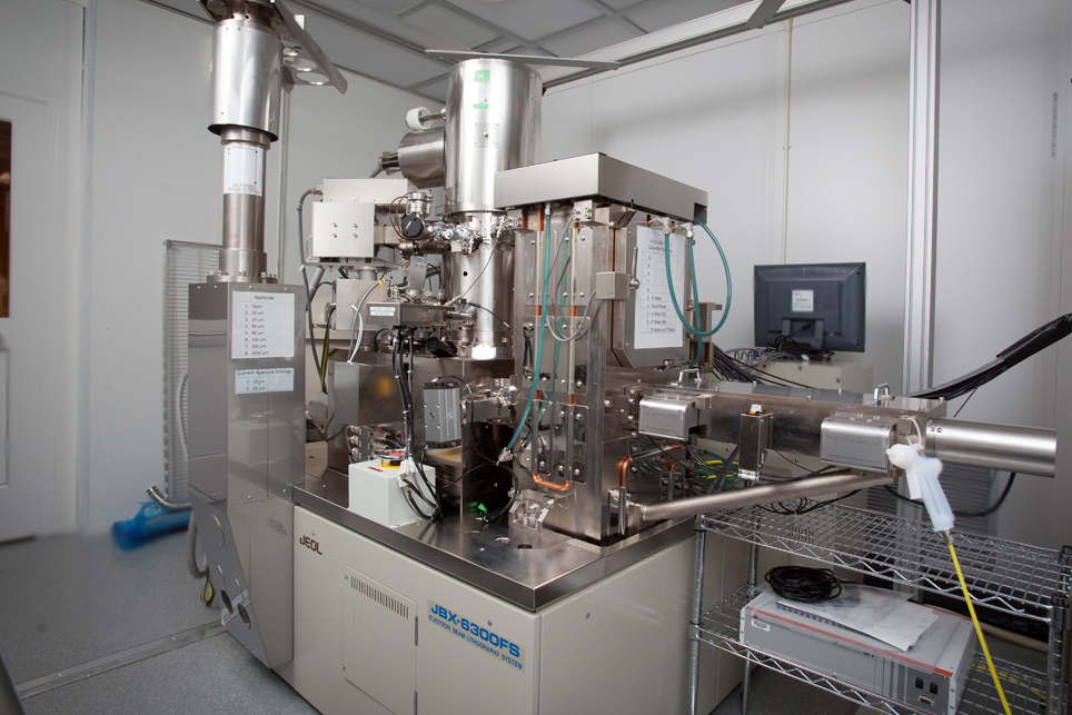
The JEOL 6300 is a high resolution 100KeV electron beam lithography system.
The unique capability of the JEOL 6300 is that a fifth lens can be used to get a smaller beam spot size and write sub-10 nm features. This is the high resolution writing mode. Writing without the 5th lens in 4th lens mode is called the high speed writing mode.
The tool can accommodate pieces as small as 5mm up to 150mm wafers.
When should I use the JEOL 9500 or the JEOL 6300?
The answer is it depends on what you are making. The 9500 has better overlay accuracy than the 6300 high speed mode (lens 4), and better stitching accuracy for large patterns. The 9500 has higher clock speed and larger field size than the 6300, so large patterns will be written faster at the same beam current. The 6300 also has a slower primary deflector than the 9500. The 6300 has better resolution in high resolution mode (lens 5) , but the field size is much smaller.
So in general, use the 9500 for large patterns and for excellent stitching accuracy. Use the 6300 for smaller patterns with the smallest feature sizes, as small as sub-10 nm. To make the best decision, compare your resolution, overlay and stitching requirements to the machine specifications listed on the tool web pages, and consult with the e beam staff.
See the Computing page for Layout BEAMER instructions.
- Overlay Accuracy in High resolution writing mode: less than or equal to +/- 20 nm; in High speed writing mode: less than or equal to +/- 35 nm
- Field Stitching Accuracy in High resolution writing mode: less than or equal to +/- 20 nm; in High speed writing mode: less than or equal to +/- 30 nm
- Beam current: 30 pA to 20 nA; Minimum beam size: less than or equal to 2.9 nm at 30 pA, in high resolution writing mode at 100 kV
- Beam positioning unit (pixel size) in High resolution writing mode 100 kV: 0.125 nm; in High speed writing mode 100kV: 1 nm
- Beam scanning step size in High resolution writing mode 100kV: 0.125 nm × N, where N = 1,2,4,6,8,…,254 (1 and even number)
- Beam scanning step size in High speed writing mode 100kV: 1 nm × N, where N = 1,2,4,6,8,…,254 (1 and even number)
- Beam scanning clock rate: 50 MHz
- Writing area: 150 mm × 150 mm
- Auto loader: Automatic 10 cassette loading system
- Writing field size in High resolution writing mode 100kV: Up to 62.5 µm × 62.5 µm; in High speed writing mode 100kV: Up to 500 µm × 500 µm