
Tool Location
122
Training
General photolithography training is required to use the e-beam spinners, hot plates and tools.
In-person training by staff is required to use the JEOL 9500. Please request training by contacting the tool manager(s) or sending an email to ebeam@cnf.cornell.edu.
If you're going to need alignment, read the requirements at https://www.cnfusers.cornell.edu/ebeam_alignment BEFORE DESIGNING ANY DEVICE. Not following these instructions may make alignment impossible.
Compatibility:
Additional Restrictions
- Fully baked resists only; do not load samples with unbaked resist or glue or anything that may degas.
Manager
Backups:
Body
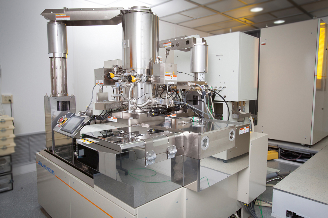
The JEOL JBX-9500FS Electron Beam Lithography System can load substrates ranging from 10 mm pieces up to 300 mm wafers and write features less than 10 nm in size. It has a 100 kV accelerating voltage, a 100 MHz clock and a 1 mm × 1 mm write field.
Capabilities
- Accelerating Voltage: 100 kV
- Field Size: 1 mm
- Writing Speed: 100 MHz
- Sample Size: Small pieces to 300 mm wafers
- Minumum beam diameter: 3.2 nm
- Minimum Feature Size: 6 nm
- Maximum beam current: 100 nA